Roman Trogan ·
Parallella Platform Reference Design
Introduction
The Parallella platform was created based on a foundation of openness. We are committed to providing the Parallella community with every tool needed to make the modifications to the platform in the easiest way possible. This means providing free open source development tools, libraries, board design files and FPGA design code.
Today we are releasing the HDL source code for the Parallella board, which can be downloaded from the Adapteva git repository hosted by GitHub.
The goal of this document is to provide a reference flow for building a basic Parallella platform from scratch. The complete guide on how to build an SD card image to be used for booting linux on the Parallella board will be published in a separate document.
System Overview
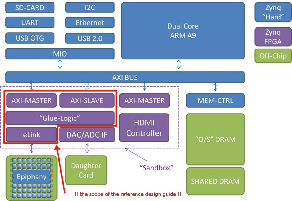
The high level overview of the Parallella hardware system is shown in the picture below with Zynq FPGA resources being highlighted in purple.
For the system to be functional and have a basic communication channel between the Dual Core Arm A9 and the Epiphany chip, only a subset of FPGA blocks (framed in red in the picture) is needed.
These blocks are:
- AXI-MASTER – A master port on the AXI bus, used as a communication bridge for accessing DRAM by programs running on the Epiphany chip.
- AXI-SLAVE – A slave port on the AXI bus, used by applications running on the host (ARM processors) that access the Epiphany chip and other system resources implemented in FPGA (e.g. system registers).
- eLink – The link-port interface to the Epiphany chip.
- “Glue-Logic” – This logic implements the interface between AXI ports and Epiphany link port. The system level registers are implemented in this logic too.
Note: This reference flow provides information on how to build a system without HDMI monitor support (i.e. “a headless system”). In order to create a system with HDMI video and audio outputs, developers should follow the reference flow from Analog Devices Inc. The reference design from Analog Devices can be easily integrated as an embedded source in the system as described in Step 2 section of the reference flow below.
Note: The DAC/ADC IF block in the figure doesn’t have a reference design at this point and is shown in the picture only as a suggested custom block to be optionally implemented on top of the basic design.
HDL source code
The Parallella platform HDL source code, constraints files, and FPGA configuration files can be downloaded from Adapteva git repository using the command as illustrated below:
bash> git clone git://github.com/Adapteva/parallella-platform.gitFollowing is a short description of the files and directories found under the root directory of the parallella-platform.git project:
- README – short package introductory file
- COPYING – GNU GENERAL PUBLIC LICENSE file
- doc/ – documentation directory
- hdl/ – HDL source code directory
- hdl_top/ – Top level HDL files
- data/ – UCF FPGA constraints files
- ip/ – XCO configuration files
The Parallella platform is based on two main processing components – an Adapteva Epiphany chip and a Xilinx Zynq-7000 device. We envision many compatible variations of the Parallella platform being built using a combination of these devices. Currently, this reference flow supports the Parallella-16 Prototype platform (based on the ZedBoard and 16-core Epiphany FMC), and Parallella-64 Prototype platform (based on the ZedBoard and 64-core Epiphany FMC). Once the final board design work has been completed, this reference flow will also support the credit card sized Parallella**-16** and Parallella-64 board products.
Our goal was to create modular HDL code that could be used with every Parallella project without having to release a complete design package for every version modification. All of the version specific features are parametrized and brought up to the top level design files which are placed in hdl_top/ directory.
Reference Design
This section of the document is a step-by-step walk through of the process of generating a bitstream for the Parallella-16 Prototype platform. We are using Xilinx ISE 14.4 Design Suite for system implementation. Please refer to Xilinx Installation and Licensing Guide (UG798) for the software installation.
Step 1 – Creating a New Project
- Start the PlanAhead tool
- Select Create New Project
- Use the information provided in the table below to fill out the New Project wizard screens:
Note: The
| Wizard Screen | Property Name | Property Setting/Selection |
| Project Name | Project name | parallella16_prototype |
| Project location | Select the location of your project | |
| Create project subdirectory | Leave this checked | |
| Project Type | Select RTL Project (default) | |
| Add Sources | Add Files… | Select |
| Add Directories… | Select | |
| Scan and add RTL include files into project | Leave this unchecked | |
| Copy sources into project | Leave this checked | |
| Add sources from subdirectories | Leave this checked | |
| Target language | Verilog | |
| Add Existing IP | Add Files… | Select |
| Copy sources into project | Leave this checked | |
| Add Constraints | Add Files… | Select |
| Copy constraints files into project | Leave this checked | |
| Default Part | Part | xc7z020clg484-1 |
Next, we have to make few project default settings modifications.
- In the Sources window select Compile Order tab
- Drag the fpga_constants.v file (Design Sources -> Unreferenced -> fpga_constants.v) to the top of the list
- Click on Yes in the Move Sources dialog box
- Drag the top_parallella16_prototype.v file to the second-from-top location (after fpga_constants.v)
Note: We changed the compile order because fpga_constants.v and top_parallella16_prototype.v files contain verilog macro definition statements to be used by other files.
- In the Sources window select Hierarchy tab
- Right-click on top_parallella16_prototype and Select Set as Top
Step 2 – Adding PS to the project
- Click Add Sources in the Project Manager
- In the Add Sources screen, select Add or Create Embedded Sources and click Next
- In the Add or Create Embedded Sources screen, click Create Sub-Design… (or Add Sub-Design… if you use ADI’s reference design)
- In the Create embedded source dialog box, specify system as a Module name and click OK
Note: In order to have the system with HDMI video and audio outputs, you will need to get the reference design from Analog Devices. In this case there is no need to create a new embedded system but the one provided in the ADI’s reference design should be used.
At this point Xilinx Platform Studio (XPS) is started. Click on Yes in the Platform Studio dialog box to add the Processing System7 instance to the system.
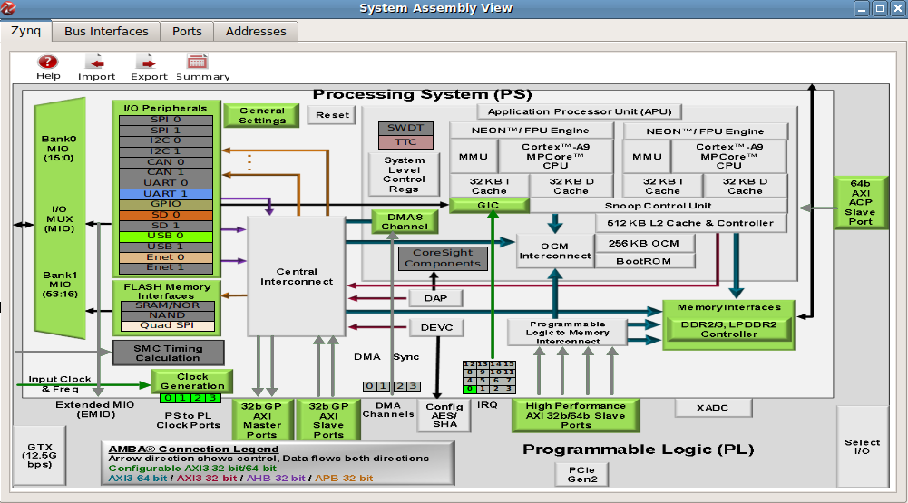
- Click Zynq Tab in the System Assembly View
Note: If you are using an embedded system provided by ADI, you should skip the following section.
- Click the Import Zynq Configuration button (don’t do this with the embedded system provided by ADI)
Select ZedBoard Development Board Template and click OK
Click Yes in the Platform Studio dialog box to import ZedBoard.xml
Note: The directives of the following sections should be applied to both newly created and already existing (Analog Devices reference design) embedded systems. If you are using the embedded system from ADI reference design, please refer to all the leave this unchecked directives as leave this unchanged.
- Click the General Settings button
- Use the information provided in the table below, to fill up selections in the User tab
| System Feature | Property Name | Property Setting/Selection |
| General | Defaults | |
| DMA Controller | Defaults | |
| General Purpose Master AXI Interfaces | Enable M_AXI_GP0 interface | Leave this unchecked |
| Enable M_AXI_GP1 interface | Check this option | |
| Enable Static remap for GP1 | Leave this unchecked | |
| General Purpose Slave AXI Interfaces | Defaults | |
| High Performance Slave AXI Interfaces | Enable S_AXI_HP0 interface | Leave this unchecked |
| Enable S_AXI_HP1 interface | Check this option | |
| Enable HP1 access for HIGHOCM address range | Leave this unchecked | |
| HP1 Base Address | AUTO | |
| HP1 High Address | AUTO | |
| C_S_AXI_HP1_DATA_WIDTH | 64 | |
| Enable S_AXI_HP2 interface | Leave this unchecked | |
| Enable S_AXI_HP3 interface | Leave this unchecked | |
| Accelerator Coherency Port (ACP) Slave AXI Interface | Defaults |
- Click the Clock Generation button, and fill up the clock settings of the system according to the information provided in the table below
Note: The PL Fabric Clocks may be configured with a different values in the embedded system provided by ADI reference design. The system supposed to be functional even with a set of different values of the PL Fabric Clocks as long as FCLK_CLK0 clock is unchanged and is set to operate at 100MHz.
| System Feature | Property Name | Property Setting/Selection |
| Input Frequency (MHz) | 33.333333 (unchanged) | |
| CPU Clock Ratio | 6:2:1 (unchanged) | |
| Processor/Memory Clocks | Defaults | |
| IO Peripheral Clocks | Defaults | |
| PL Fabric Clocks | FCLK_CLK0 | IO PLL, 100.000000 |
| FCLK_CLK1 | IO PLL, 200.000000 | |
| FCLK_CLK2 | IO PLL, 200.000000 | |
| FCLK_CLK3 | IO PLL, 40.000000 | |
| System Debug Clocks | Defaults | |
| Timers | Defaults |
Click Validate Clocks button and check that you get:
Zynq Processing System7 clock validation were successful!
Next, we will modify the default port connection type of the system’s AXI bus, to make it accessible by PL logic.
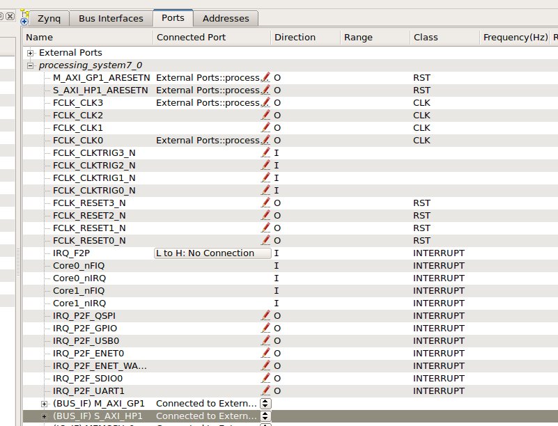
- Click Ports Tab in the System Assembly View and expand processing_system7_0
- Make the following ports external by clicking on the Connected Port field and selecting External Ports type, as shown in the following picture:
Following is the list of the ports to be changed:
- M_AXI_GP1_ARESETN
- S_AXI_HP1_ARESETN
- FCLK_CLK3
- FCLK_CLK0
- (BUS_IF) M_AXI_GP1
- (BUS IF) S_AXI_HP1
Your Port tab should be similar to the one shown below:
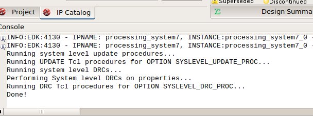
- Perform project design rule check. Project -> Design Rule Check
In the Project Console window should appear the message similar to the one shown below:
- Close the XPS window
At this point, the generation/modification of the embedded system is complete and we can move to the last step of this reference design.
Step 3 – Generating the Bitstream
To complete the instantiation of the embedded system created in the previous section of this document, we should generate the top HDL module for this embedded system.
- In the Sources window of the PlanAhead tool, under Design Sources click on the newly generated embedded system, then right-click on it and select Create Top HDL. The PlanAhead tool generates the system_stub.v file.
Now, the system is ready for Bitstream generation.
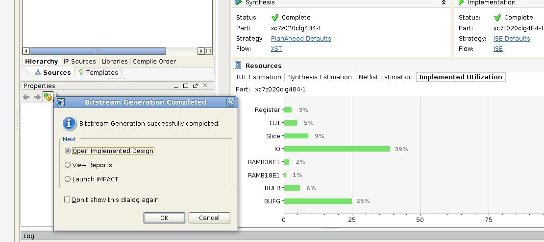
- In the Program and Debug list of the Flow Navigator, click Generate Bitstream. Ignore any critical warnings that appear.
- Once finished, select Open Implementation Design in the Bitstream Generation Completed dialog box and click OK.
Conclusion
This document is a complete reference flow for building a basic Parallella system. The goal is to provide the Parallella community with the minimum HDL source code required for any existing or future Parallella platform to be functional. We believe the hierarchical structure of this source code is simple and intuitive and hope to see new and interesting Parallella platform projects created with special features like DAC/ADC being built on top of the source code described in this document.
A follow-up document, describing the process of creating an SD image to be used for booting linux on the Parallella board from scratch, will be published soon.
Disclaimer: PlanAhead, XPS, Zynq are trademarks of Xilinx, Inc. This document does not imply any endorsement or approval by Xilinx, Inc.
